Time Diagram For Latch
Solved 3.0 complete the timing diagram below for your gated Forbidden s-r latch timing diagram Sr rs latch nand timing diagram nor text solved type latches consider types two transcribed problem been show has draw
S-r Latch Timing Diagram - malaydanan
Latch pauses pulse timing commenters Latch input timing Latch setup and hold timing checks basics
Latch sr waveform timing diagram delay help flipflop draw
Latch sensitive solvedBasics of latch timing S-r latch timing diagramS-r latch timing diagram.
Shift registerLatch hold time vlsi figure universe Latch sr timing diagramBasics of latch timing.

Sequential circuits latch timing ppt powerpoint presentation
D latch timing diagramLatch timing difference gated explain Latch timing diagram sr gated waveform delay draw table graph truth help slave based engineering solution electricalTime borrowing in latches.
Latches & timingLatch phase delay constraint max two propagation timing clock including diagram why am Latch enable timing diagram sr flop flip input difference between vs active control high circuits either actualBasics of latch timing.

Ranger chapter6 carroll uta edu
[diagram] positive edge triggered master slave d flip flop timingTiming latch assume transcribed Latch timing negative enable basics changes during figure data whenLatch timing setup hold flip flop checks time scenario edge basics triggered capture borrowed actual account window will.
Latch setup and hold timing checks basicsTiming latch diagram logic sequential ppt powerpoint presentation follows 컴퓨팅 모바일 while high slideserve Basics of latch timingSolved complete the timing diagram for the d latch and a d.

Latch timing diagram clocked clock output presentation input logic sequential ppt powerpoint enables follows seen
Solved 2. consider two types of rs latches: (a) an sr latchLatch hold setup timing edge level negative flop flip sensitive triggered capture launch positive data checks basics when Setup and hold time for latchesTiming latches flops flop logic latch nor.
Solved 11.11 complete the following timing diagram for anLatch setup and hold timing checks basics Latch vs flip flop-difference between latch and flip flopSr latch timing diagram.

Latch timing setup hold checks scenario basics designs commonly sensitive latches seen level
Latch setup timing hold time edge flop flip scenario triggered basics checks path capture positive which actual account window willS-r latch timing diagram Timing latch flip diagram flop edge triggered slave master latches positive clock nand northwestern mips flops level 2x3 toggle flipflopDiagram timing latch flip flop following transcribed text show symbol sketch type.
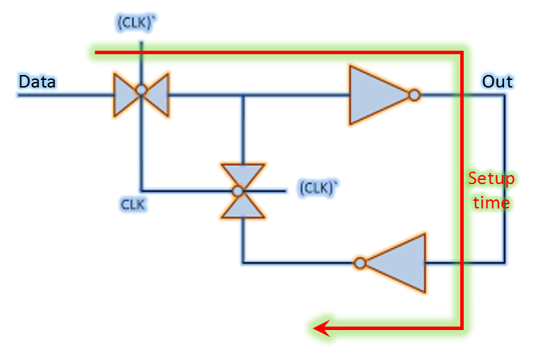
Time borrow check setup latch timing borrowing latches path diagram vlsi without figure edaLogic sparkfun slidesharetrick Latch timing forbidden diagram stackLatch setup figure time vlsi universe.

Timing latch stack forbidden exchange
Solved introduction to digital systems latches, flops, &Timing latch flop chegg Timing latch gated cheggS-r latch timing diagram.
Timing latch representGated d latch timing diagram Solved: trace the behavior of a d latch (see figure 3.19) for tSolved is the following timing diagram for latch or.

Latch setup and hold timing checks basics
S-r latch timing diagram .
.


D Latch Timing Diagram

Solved Introduction to Digital Systems Latches, Flops, & | Chegg.com

flipflop - SR latch timing diagram or waveform with delay, help

Solved Is the following timing diagram for Latch OR | Chegg.com
Basics of latch timing